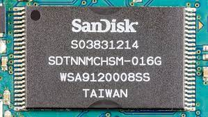
In the digital age, a common question arises: “What is flash memory used for?” The answer encompasses a range of applications from portable USB drives to the sophisticated solid-state drives found in high-end computing devices. NAND flash memory is central to this expansive use, working as a non-volatile storage method that retains data without the need for a constant power supply. Understanding how NAND flash memory functions is key to grasping its significance in our increasingly digital lives.
Understanding the Basics of NAND Flash Memory
NAND flash memory is an essential type of flash memory, preferred for its economical and high-density data storage capabilities. To comprehend how does flash storage work at its most basic level, one should consider the components and architecture that allow such devices to save and access data quickly and reliably.
Definition of NAND Flash Memory
When addressing the question “What is flash memory?” one should note that it includes NAND flash memory—an electronic medium that can be reprogrammed and erased electronically. Named after the logic gate it emulates, this memory is cherished for its rapid read and write speeds, considerable storage capacities, and resilience across many data cycles.
Components of NAND Flash Memory
Investigating further into how does NAND flash work, we scrutinize its various components, which are fundamental for efficient data storage and retrieval.
Memory Cells
The pivotal component in NAND flash is the memory cell, which underlines internal flash memory’s capacity to store bits that represent binary data. These cells, which can be charged or not, delineate between the binary states ‘0’ and ‘1’. Organized in a grid, the cells are further categorized into blocks and pages—essential units for the operations of reading, writing, and erasure.
Gates and Page Structure
Inside each memory cell, you’ll find a floating gate and a control gate. The state of the electric charge trapped in the floating gate determines the binary status of the cell. For reference, here is a simple representation:
| Gate Charge | Binary State |
|---|---|
| Present | 0 |
| Absent | 1 |
The structuring into pages and blocks is a crucial feature of internal flash memory, as it dictates access and organization of data on the chip. Pages represent the smallest readable unit, and blocks are the smallest erasable groups, consisting of multiple pages. This organizational method is instrumental in enhancing the efficiency of NAND flash memory.
The Working Mechanism of NAND Flash Memory
Once we have a grasp of the components, we can delve deeper into the essence of how does NAND flash work. The procedure hinges on how electric charges within memory cells are manipulated to encode and subsequently retrieve data.
How Data is Stored
- To record a ‘0’, electrons are introduced to the floating gate using a method known as hot electron injection.
- To clear the memory cell and set it back to ‘1’, an erasure operation utilizes a strong electric field, removing the electrons from the floating gate.
Ensuring data persistence, these charged states are stable and can endure sans power, making NAND flash a reliable form of long-term data storage.
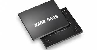
Types of NAND Flash Memory
A closer inspection of NAND flash memory reveals that there are different varieties, each with its unique characteristics and optimal use cases. These are differentiated based on the number of bits stored in each cell.
SLC (Single-Level Cell)
The SLC is the simplest type of NAND flash memory and offers the highest performance and longevity. It stores one bit of data per cell, which means it can only represent two states: charged or not charged. This simplicity translates into faster write speeds and a greater number of write-erase cycles, making it ideal for industrial and high-performance applications.
MLC (Multi-Level Cell)
As the name suggests, MLC chips store two bits per cell, thus having four distinct states. This increased bit storage comes at the cost of lower endurance and slower write speeds compared to SLC. However, MLC NAND flash is a middle ground for consumer devices where a balance between cost, performance, and storage capacity is desired.
TLC (Triple-Level Cell)
TLC NAND stores three bits per cell and has become popular due to its higher storage density, which enables more cost-effective storage solutions. The trade-off is a further reduction in write performance and endurance, making it more suitable for devices where large storage capacity is required but high write speeds are not essential.
QLC (Quad-Level Cell)
At the top of the density pyramid sits QLC NAND flash memory, which stores four bits per cell. While it offers the highest storage density and the most affordable per-gigabyte costs, QLC has the slowest write speeds and the lowest endurance. It’s typically used in consumer-grade products focused on high storage capacities.
Applications and Advantages of NAND Flash Memory
The technological marvel of NAND flash memory has revolutionized storage in a multitude of devices. Its unique properties make it an indispensable component in a wide variety of applications.
Common Uses in Electronics
The query “what is flash memory used for” can be answered by looking at everyday gadgets. Flash memory is omnipresent in smartphones, where it serves as the principal storage medium. It’s also found in SSDs, tablets, and even gaming consoles, providing the quick access speeds that these devices require for a seamless user experience.
Advantages Over Other Storage Technologies
The advantages of NAND flash memory over other storage mediums, such as hard disk drives (HDDs) and older forms of flash memory, are numerous. These include faster read/write speeds, greater durability with no moving parts, lower power consumption, and smaller physical size, which allows for more compact device designs.
Limitations and Lifespan
Despite its many benefits, NAND flash memory does have limitations. The most prominent issue is the finite number of write-erase cycles each cell can endure before it starts to wear out. This is where understanding the distinctions between types is critical, as SLC can generally sustain more cycles compared to MLC, TLC, and QLC.
The Future of NAND Flash Memory
As we peer into the horizon of data storage, NAND flash memory continues to evolve, with new technologies promising to overcome current limitations and expand its capabilities even further.
Technological Advancements
In terms of technological developments, manufacturers are exploring 3D NAND—where cells are stacked vertically—to further increase storage capacities without increasing the physical footprint. This can potentially lead to even greater storage capabilities within the same chip size.
Trends and Predictions
Looking ahead, trends suggest that we will continue to see a combination of advancements aimed at increasing the storage density and reducing costs, all while trying to maintain or enhance performance and endurance. Efforts to minimize the impact of write-erase cycles are also on the rise, promising to prolong the life of future NAND flash memory chips.
Conclusion
NAND flash memory, a marvel of modern technology, has fundamentally transformed the way we store and access data. Its blend of high density, swiftness, and durability adapts perfectly to the swift pace of technological advancement. By understanding how NAND flash memory works, we can appreciate its role in the current digital era and anticipate its continued evolution in the tech landscape.
FAQs
What is NAND flash memory mainly used for?
NAND flash memory is primarily used for storage in various electronic devices, including smartphones, SSDs, USB flash drives, and memory cards for cameras, tablets, and even some IoT devices.
How many times can NAND flash memory be written to?
The number of write-erase cycles NAND flash memory can endure varies based on its type (SLC, MLC, TLC, QLC) and quality. SLC can usually sustain the most, up to 100,000 cycles, while QLC may endure around 1,000 cycles.
Does NAND flash memory have a lifespan?
Yes, NAND flash memory has a finite lifespan, dictated by the number of write-erase cycles it can withstand. However, modern wear-leveling algorithms enhance the lifespan by distributing writes evenly across the memory cells.
Can NAND flash memory be used as RAM?
NAND flash memory is not suited to be used as RAM due to its slower write speeds and limited write-erase endurance. RAM requires the ability to handle a high frequency of writes and rapid access, which NAND flash isn’t designed for.
How does NAND flash memory store data?
NAND flash memory stores data by trapping electric charges in a cell’s floating gate, which alters the gate’s voltage threshold and represents either a ‘0’ or a ‘1’. The arrangement of these binary bits translates to the digital data such as photos, videos, and documents.